Terahertz metamaterials and their applications in imaging
terahertz; metamaterial; metasurface; imaging
Abstract
Electromagnetic metamaterials have attracted more and more research interest due to their exotic physical properties and important applications in manipulating electromagnetic waves . In this paper, the research progress in terahertz metamaterials and their applications in imaging was reviewed: firstly, the research of terahertz metamaterials was overviewed, and tunable and reconfigurable terahertz metamaterials as well as terahertz digitally coding and field -programmable metamaterials were discussed in detail; then, the applications of terahertz metamaterials in imaging were illustrated, including terahertz imaging technologies based on metasurface lenses, metamaterial absorbers, reconfigurable metasurfaces, and field-programmable metasurfaces; finally, the prospects of terahertz metamaterials and their applications in imaging were provided.Reconfiguration and in telligence of the functions will be an important development direction of terahertz metamaterials, and the emerging information metamaterials which integrate meta materials and information technology will enable more efficient and convenient terahertz imaging.
Introduction
Electromagnetic metamaterials (metamaterial), also known as new artificial electromagnetic media, metamaterials, etc., are characterized by arranging artificial unit structures (artificial atoms) with sub-wavelength scales in a periodic or non-periodic manner, and then obtaining materials beyond the limits of natural materials. Electromagnetic properties, such as negative refractive index, zero refractive index, ultra-high refractive index, high-frequency magnetic response, etc.
Since the 1990s, research on the basic theory, functional devices and engineering applications of electromagnetic metamaterials has aroused extensive research interest in the fields of physics, information and materials.
Based on the designable electromagnetic parameters and distribution of metamaterials, researchers have developed various new devices such as metamaterial cloaks, lenses, and antennas.
According to the field localization and field enhancement characteristics of metamaterials (this effect is especially significant in surface plasmon metamaterials) and subwavelength scale characteristics, novel metamaterial sensing and imaging devices have been developed, which can effectively improve sensor sensitivity and imaging resolution.
With the proposal and realization of digital coding and programmable metamaterials, the characterization and design of metamaterials are carried out in a binary digital way (that is, digital 0 and 1), which promotes the integration of metamaterials and information technology, making the new system superhuman. Material imaging systems and communication systems made possible.
The terahertz frequency region is between microwave and far-infrared in the electromagnetic spectrum, and is usually defined as electromagnetic radiation between 0.1 and 10 T Hz. With the rapid development of terahertz sources and detectors and the continuous development of terahertz functional devices, terahertz science and technology have achieved vigorous development in recent years.
Terahertz technology has great application prospects in material characterization, security inspection, biomedical imaging and communication.
Among them, in terms of imaging, compared with microwave and millimeter wave frequencies, terahertz imagers will have higher spatial resolution, and compared with optical imaging, terahertz radiation has better penetration, so it can obtain more Multiple depth information. At the same time, since this is a kind of non-ionizing radiation, it has better biological safety, so the application of terahertz imaging has been widely concerned.
Terahertz metamaterials and metasurfaces have broad application prospects in terahertz imaging systems due to their sub-wavelength unit scale and flexible manipulation of electromagnetic wave amplitude, phase and polarization characteristics.
This paper first introduces the research overview of terahertz metamaterials, focusing on the research progress of tunable and reconfigurable terahertz metamaterials, terahertz digital coding and field programmable metamaterials.
On this basis, the application of terahertz metamaterials in the field of imaging is described, including terahertz imaging technologies based on metasurface lenses, metamaterial absorbers, reconfigurable metasurfaces and field programmable metasurfaces. Finally, the development trends of terahertz metamaterials and their imaging applications are discussed.
1. Terahertz electromagnetic metamaterials
1.1 Research overview of terahertz metamaterials
In the 1990s, Sir John Pendry of Imperial College of Technology proposed to use the method of equivalent medium parameters to construct low-frequency negative permittivity and negative magnetic permeability, which was verified experimentally at microwave frequencies by the team of Professor Smith of Duke University in the United States. Since then, the research on electromagnetic metamaterials has continued for more than 20 years.
With the use of micro-nano processing technology, metamaterials in the terahertz, infrared, and visible light bands can also be realized in the laboratory.
In particular, terahertz magnetic metamaterials have broken through the limitations of natural materials and obtained magnetic responses at high frequencies. As shown in Figure 1(a), the split-ring resonator (SRR) structure produces a magnetic response under the excitation of a magnetic field component perpendicular to the torus.

Fig.1Schematic diagrams of terahertz magnetic metamaterial (a) and functional device (b)
For the SRR array whose outer ring size and period length are 32 μm and 44 μm, respectively, its magnetic resonance frequency is about 1.0 T Hz.
Negative or ultrahigh refractive indices can also be obtained based on terahertz metamaterials. At the same time, researchers have developed various new terahertz metamaterial devices, including cloaks, absorbers, modulators, and optical switches, to regulate the propagation properties of terahertz waves.
As shown in Fig. 1(b), a multi-layer terahertz absorber was designed using metal wire resonators and lossy dielectrics, and a broadband high-efficiency absorber with an absorption rate of more than 95% was achieved in the 0.5T Hz frequency range (center The frequency is 1.06T Hz). Therefore, terahertz metamaterials greatly enhance people’s degree of freedom in manipulating terahertz waves.
Electromagnetic metasurfaces, as a two-dimensional form of metamaterial, have attracted extensive research interest.
Compared with three-dimensional metamaterials, metasurface units have deep subwavelength thicknesses. Its manipulation of electromagnetic waves does not depend on the phase accumulation in space, but on the basis of the phase gradient (discontinuous distribution) between adjacent units to realize the manipulation of the properties of electromagnetic wave front, amplitude, phase and polarization.
Therefore, the use of metasurface solutions is beneficial to the design of ultra-light, ultra-thin, and easily conformable terahertz devices, such as metasurface anomalous reflection/refraction devices, polarization converters, and low-scattering devices. Figure 2(a) is a schematic diagram of the structure of the beam anomalously deflecting metasurface.

Fig.2 Schematic diagrams of terahertz metasurface devices(a)anomalous deflection of terahertz beam;(b)linear polarization converter;(c)low‐scattering metasurface
Its unit is composed of 8 kinds of resonators with different phases, which can achieve 360° phase coverage. Through the combination of a metasurface and a pair of orthogonal gratings, the abnormal deflection and efficient polarization conversion of transmissive terahertz linearly polarized waves can be realized.
As shown in Fig. 2(b), a linearly polarized wave conversion device is designed using a similar I-shaped unit structure.
As shown in Figure 2(c), by designing the arrangement of metasurface units with different amplitude and phase responses, ultra-low scattering of terahertz beams (reduced radar cross section, ie reduced RCS) and electromagnetic stealth can be achieved. Therefore, terahertz metasurface devices can achieve flexible manipulation of terahertz beams and have the advantages of light weight and easy conformality.
1.2 Tunable and reconfigurable terahertz metamaterials
The electromagnetic properties of metamaterials usually depend on the artificially designed unit structure, so once the metamaterial structure is fixed, its electromagnetic properties will also be fixed.
Tunable and reconfigurable metamaterials with the characteristics of multi-function and adjustable operating frequency have attracted extensive research interest.
The typical tunable physical mechanism of metamaterials is to change the electromagnetic properties (such as permittivity and magnetic permeability) of constituent materials or surrounding media (such as substrate materials) by changing temperature, external electric field or magnetic field, etc., in order to realize the work of metamaterials The purpose of frequency and transmission properties can be tuned.
Commonly used materials include superconducting materials, graphene, liquid crystals, phase change materials, metal titanates, and magnetic materials.
Chen et al designed a terahertz SRR metamaterial on a 180nm-thick YBCO (YBa2Cu3O7-δ, δ=0.05) superconducting film, whose terahertz resonance frequency and transmission properties are adjustable with temperature.
Its working principle is that the conductivity of superconducting thin films is temperature-dependent, which leads to the temperature-tunable electromagnetic resonance characteristics of SRR metamaterials (see Figure 3(a)).
Graphene is a two-dimensional material whose surface conductance can be tuned by changing the chemical potential, so it can also be applied to tunable metamaterials. The metamaterial device shown in Figure 3(b) covers a single layer of graphene on the surface of a zero-refractive index metamaterial, and the tunable Goos-Hänchen effect is realized by electrically adjusting the Fermi level of graphene.
Graphene-based metamaterial absorbers, optical switches, and phase shifters have also been widely reported.
The optical properties of nematic liquid crystal materials are anisotropic. For example, the terahertz normal and anomalous refractive indices of LC1852 are 1.56 and 1.89, respectively. Therefore, in terahertz tunable metamaterials, terahertz phase shifters and terahertz beam scanning devices have potential applications.
The liquid crystal/metamaterial tunable absorber is shown in Figure 3(c), and its structure is composed of a resonant unit, a liquid crystal layer and a metal backplane layer. By adjusting the orientation of the liquid crystal through electrical bias, a 30% absorption adjustment can be achieved at a frequency of 2.62 T Hz. In addition, terahertz glass slides can be designed using liquid crystal materials, and their structures include: quartz substrates, metal gratings, sulfonic acid azo dyes, liquid crystals, and graphite electrodes.
By adjusting the bias voltage to change the phase difference between the o-light and e-light, the polarization state of the outgoing light can be dynamically changed to obtain linearly polarized, circularly polarized, and elliptically polarized THz light, respectively.
Vanadium dioxide (VO2) is a typical phase change material. Its metal-insulator phase transition temperature is about 68 °C, and it can be induced by applying a strong electric field, laser or pressure.
The terahertz permittivity of insulating VO2 is about 9. As the temperature increases, its conductivity increases, and the conductivity of epitaxial VO2 film can reach 105 S/m, so the complex permittivity needs to be considered.
VO2 has been widely used in tunable metamaterial devices.
Figure 3(d) is a schematic diagram of the structure of the VO2/metamaterial filter. The research results show that as the temperature rises from 25°C to 90°C, the resonant filter frequency blue-shifts from about 0.41THz to about 0.54THz.
Hillman et al. designed a broadband terahertz phase shifter using VO2, which achieved a phase shift of more than 300° in the frequency range of 220–250 GHz, which can be applied to terahertz beam steering including beam scanning. Metamaterials and devices based on dielectric materials (such as metal titanates) also have the characteristics of being tunable with temperature.
Magnetic materials also have broad applications in tunable metamaterials. Bi et al. designed a magnetic metamaterial unit using Mn‐Zn microwave ferrite material, and achieved a thermally adjustable negative refractive index by compounding it with a metal wire unit (ferrite has a ferrimagnetic‐paramagnetic phase transition, so Its magnetic response properties are temperature dependent).
In addition, magnetically tunable broadband microwave filters can be realized using ferrite-based metamaterials. Figure 3(e) shows a schematic diagram of a magnetically tunable terahertz modulator. Its main components include a terahertz metamaterial layer and a magnetic fluid layer, where the magnetic fluid layer is Fe3O4 nanomaterials.
The results show that when the intensity of the magnetic field bias is 194 mT, the modulation depth of the terahertz transmission amplitude can reach 34%.
Reconfigurable metamaterials generally refer to the reconstruction or adjustment of their properties through the reconstruction of the geometric structure of metamaterials. Common approaches to reconfigurable metamaterials include microelectromechanical systems (MEMS) technology and deformation technologies (such as thermal, stress-induced deformation).
Figure 4 (a) is a terahertz reconfigurable metamaterial based on MEMS technology. Its unit structure is composed of two parts, namely a fixed split ring and a movable split ring.
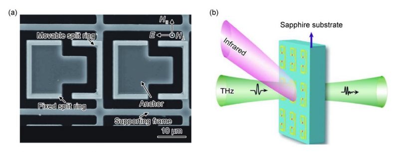
Fig. 4 Schematic diagrams of terahertz reconfigurable metamaterial (a)and active metamaterial (b)
The latter is placed on a movable platform, and Its position can be controlled in real time by the micromechanical actuator, and then the dynamic regulation of the resonance properties of the metamaterial unit can be realized.
The results show that as the distance between the fixed ring and the movable ring changes, the magnetic resonance frequency of the metamaterial shifts significantly, and the equivalent permeability curve also shifts accordingly.
It is also a common method in MEMS technology to change the height of the cantilever beam through the driving voltage, and then adjust the geometric parameters and resonance frequency of the metamaterial unit. Changing the shape of metamaterials based on thermal or stress effects can also achieve reconfiguration of metamaterials.
Usually, metamaterials composed of materials with different thermal conductivity are heated and lowered to make them bend, or the substrate with good ductility is stretched to change the geometric parameters of metamaterials.
In addition, active elements or functional materials, such as diodes, semiconductor materials, graphene, etc., can be introduced into metamaterial units to construct active metamaterials. By applying excitation conditions such as bias voltage or optical pumping to active metamaterials, real-time regulation of the electromagnetic properties of metamaterials can be achieved, thereby achieving the purpose of manipulating terahertz beams.
As shown in Figure 4(b), the semiconductor Si (red square in the figure) is introduced into the metamaterial unit (the yellow part in the figure is metal Al). Active control of terahertz electromagnetically induced transparency can be achieved by varying the optical pump intensity and thus the conductivity of Si.
In addition, semiconductor materials (such as Si) are excited by pump light modulated by field distribution (such as spatial light modulator), since the surface conductivity of the illuminated area and the non-illuminated area are different, the corresponding terahertz phase response is also different, thus forming a specific metasurface pattern. By adjusting the intensity distribution of the pump light, the pattern reconstruction of the metasurface can be realized.
Tunable, reconfigurable, and active metamaterials make the functions of metamaterials no longer fixed, but can be regulated by external excitation, so that the working frequency of metamaterials can be adjusted or switched between different functions, so that manipulate the transmission properties of electromagnetic waves in a greater degree of freedom.
1.3 Terahertz digital encoding and programmable metasurface
Classical metamaterial systems usually use equivalent medium parameters to describe the electromagnetic properties of metamaterials, and the design of metamaterial cloaks and metamaterial lenses is mainly to design the distribution of equivalent electromagnetic parameters.
Due to the limitations of basic principles, it is difficult for equivalent medium metamaterials to integrate with information technology. Therefore, Professor Cui Tiejun of Southeast University proposed the concepts of digitally coded metamaterials and field programmable metamaterials.
The digitally coded metamaterial performs binary coding according to the difference in unit response phase (or amplitude) (for example, in 1-bit code, the digital codes corresponding to two units with phases of 0° and 180° are 0 and 1; another example is 2-bit Code, the four units with phases of 0°, 90°, 180° and 270° correspond to digital codes of 00, 01, 10 and 11). When designing metamaterials, it is only necessary to design coding patterns according to functional requirements.
As shown in Figure 5(a), the unit structure of the terahertz digitally encoded metasurface is a Minkowski structure, and its phase response is approximately linear with the unit size and can cover the range of 2π. Therefore, selecting units of different sizes can obtain 1 -bit, 2-bit and 3-bit digitally encoded metasurfaces. By optimizing the encoding pattern, single-beam, dual-beam, multi-beam radiation and RCS reduction of terahertz waves can be achieved.

Fig.5 Schematic diagrams of digitally coding metamaterials and programmable metamaterials (a)terahertz coding metasurface;(b)microwave programmable metasurface :unit cell and FPGA controlling module ;(c)phase response of the element of the terahertz programmable metasurface based on M EMS technology ;(d)schematic diagram of the coding sequence of the terahertz prog rammable metasurface
The field programmable metamaterial is to embed active elements (such as switching diodes) in the metamaterial unit, and realize the real-time adjustment of the phase response (digital code state) of the metamaterial unit by regulating the on and off of the diode; input the digital code sequence into the field programmable In the gate array (FPGA), the bias voltage is controlled by the FPGA to realize the real-time switching of the encoding pattern of the metamaterial array, thereby manipulating the far-field radiation properties of the metamaterial array (see Figure 5 (b)).
In the terahertz frequency band, the application of active components is limited by some parasitic effects, so MEMS technology or tunable materials (such as graphene, liquid crystal, etc.) can be used to achieve real-time phase adjustment.
Cong et al. designed a terahertz programmable metasurface based on MEMS technology. As shown in Figure 5(c), the phase response of the metasurface unit can be adjusted by changing the angle between the cantilever and the substrate through the driving voltage, and the phase coverage exceeds 300°, so 1-bit and 2-bit encoding units can be designed as required.
Figure 5(d) is a schematic diagram of a one-dimensional 1-bit coding sequence, that is, the coding pattern is independently regulated by column, while the two-dimensional programmable metasurface is very difficult in the terahertz band, mainly due to the high complexity of the control circuit.
Graphene-based terahertz programmable metasurfaces have attracted attention. That is, the graphene material is embedded in the unit, and the phase response of the unit is adjusted by applying a bias voltage to realize real-time switching of the encoded state.
Digitally encoded metamaterials and field programmable metamaterials are also called information metamaterials. Through the digitization of metamaterial description and design methods, the integration of metamaterials and information technology has been realized. Therefore, based on information metamaterials, digital information processing can be directly performed, and then new wireless communication systems and imaging systems can be developed.
2. THz metamaterial imaging
2.1 Overview of Metamaterial Imaging
Terahertz imaging has important applications in security inspection and detection of materials and biological tissues due to its high spatial resolution and biological non-destructive characteristics.
According to different imaging principles, it can be divided into near-field imaging and far-field imaging. The two are to collect near-field evanescent wave signals and far-field conducted wave signals for imaging.
Near-field imaging can break through the diffraction limit and obtain sub-wavelength resolution, but it has high requirements on imaging equipment and environment; far-field imaging has relatively low resolution, but has low equipment requirements and can image larger objects.
As mentioned earlier, one of the important applications of electromagnetic metamaterials is super-resolution imaging.
Imaging with a negatively refracting slab lens (“perfect lens”) can amplify the evanescent wave signal to obtain sub-wavelength imaging resolution. However, the “perfect lens” has significant loss and poor practicability.
Zhang et al. used Ag plasma lenses to achieve sub-diffraction-limited imaging at a wavelength of 365 nm, with a resolution of 1/6 wavelength. The above-mentioned super-resolution imaging is obtained in the near field, and the hyperbolic metamaterial can convert the evanescent wave into a propagating wave and obtain an image with sub-wavelength resolution in the far field.
The cylindrical cavity metalens composed of alternating Ag and Al2O3 thin films realized sub-wavelength imaging at 365 nm wavelength with a resolution of 130 nm. It is worth noting that image sensors based on metamaterial filters have also attracted numerous research interests.
The working wavelength of the metamaterial filter is related to the size. By adjusting the geometric parameters, the transmission bands of the three units are respectively in the red, green, and blue bands, so that a complete pixel image sensor applied to visible light can be formed.
Due to the sub-wavelength characteristics of the metamaterial unit, it is beneficial to reduce the pixel size and improve the resolution.
In recent years, the birth of information metamaterials provides a new imaging mechanism. Since the radiation pattern of the field programmable metamaterial can be switched in real time through the FPGA, the scattering signal of the target under different radiation patterns can be collected during imaging, and the target can be reconstructed after signal processing by the inverse scattering algorithm.
This imaging method has the characteristics of single sensor, single frequency point and no scanning. In addition, dynamic holographic imaging can also be performed by using programmable metasurfaces. If the working frequency can be extended from microwave to terahertz frequency, and then the spatial resolution can be improved, it will have important application prospects.
Of course, in the terahertz frequency band, semiconductor active components are more limited, and tunable materials are expected to replace them.
2.2 Research progress of terahertz metamaterial imaging
2.2.1 Imaging technology based on terahertz metasurface lens
Compared with traditional optical lenses, planar metasurface lenses are thinner and lighter, which is conducive to the miniaturization and integration of imaging systems. Figure 6(a), (b) are schematic diagrams of the terahertz metasurface unit structure and metasurface lens, respectively.

Fig.6 Schematic diag rams of unit cell (a) and lens (b) based on terahertz metasurface, all‐dielectric meta‐lens and the optical microscope image (c)
The metasurface unit is a metal-dielectric-metal three-layer structure with a period and thickness of 100 μm and 50 μm, respectively.
The design operating frequency of the metasurface lens is 0.84 T Hz, the focus diameter after focusing is about 1 of the wavelength. 26 times, the incident angle range up to 30° and insensitive to incident polarization.
The all-dielectric metalens and its optical microscopic image are shown in Fig. 6(c). The metalens unit is a Si column deposited on the surface of SiO2 with a size of 0. 39 λ0 (working wavelength is 118.8 μm). The focal length and radius of the metalens are both 300 λ0 and the numerical aperture is 0. 707, the maximum incident angle can reach 48° when focusing.
2.2.2 Imaging technology based on terahertz metamaterial absorber
Terahertz imaging detectors can be designed using terahertz metamaterial absorber arrays. The schematic diagram of multispectral imaging based on metamaterial absorber is shown in Fig. 7(a).

Fig.7 Schematic diagrams of terahertz metamaterial absorber imagers(a)terahertz multi‐spectral imager based on metasurface absorber arrays;(b)terahertz absorber imager based on CMOS technology
The imaging system is a bolometer matrix structure with an array size of 24 × 24, mainly composed of artificial impedance surface AIS (including metasurface MS, polymer film PP and metal ground GL) and infrared radiation layer EL.
Its design working frequency band is 0.3 ~ 0.4 T Hz, composed of 4 different pixels: 3 pixels have the same polarization sensitivity orientation, and the absorption frequency is 0 . 30 , 0.33 , 0.36 THz; the frequency of the fourth pixel is 0.33 THz, its polarization sensitivity orientation is orthogonal to the first 3 pixels.
The pixel size is 0.9 mm × 0.9 mm with a period of 1.3 mm × 1.3 mm, all have near-perfect terahertz wave absorption. During the imaging process, the metamaterial absorber absorbs terahertz energy, causing the temperature to rise, and releases heat in the form of infrared radiation (terahertz and infrared conversion), which is finally captured by the infrared detector.
This is a real-time, uncooled terahertz imaging system that is polarization sensitive. Figure 7(b) further shows a design scheme based on 180nm-CMOS process.
Its structure is composed of a terahertz metamaterial absorber and a silicon pn diode, and the designed operating frequency is 2.52 T Hz, the working principle is: after the terahertz absorber absorbs energy, the temperature rises, which causes the output voltage of the pn diode to change, and the incident terahertz radiation intensity can be measured by monitoring the voltage.
The area of the imaging sensor is 1.5 mm × 1.5 mm, and the single pixel size is 30 μm. Research shows that this is a real-time imaging device working at room temperature, and the highest detection sensitivity can reach 684 V/W.
2.2.3 Imaging technology based on terahertz reconfigurable metasurface
Figure 8 shows the imaging mechanism based on the terahertz reconfigurable metasurface. As shown in Figure 8(a), a terahertz spatial light modulator is constructed by using an 8 × 8 reconfigurable metasurface array, in which each pixel is a dynamically adjustable terahertz metasurface absorber, and its absorbing properties (including two states of high absorption and low absorption) can be adjusted in real time and independently by bias voltage.

Fig.8 Schematic diagrams of terahertz metasurface imaging systems (a)imaging system based on amplitude‐reconfigurable metasurface;(b)schematic diagram of the purephase‐hologram imaging system based on reconfigurable metasurface; (c)phase‐g radient distribution of metasurface elements ;(d)metasurface pattern for holog ram of letter “C”
The absorbing state distribution of the array (depending on the bias voltage distribution) can be controlled by FPGA.
After the terahertz beam passes through the target to be imaged, it is incident on the metamaterial spatial light modulator, and after being partially absorbed (beam modulation), it is reflected to a single-pixel detector (liquid helium-cooled Si thermal radiometer) for terahertz radiation intensity detection; Changing the pattern of the spatial light modulator, repeating the above experiment; reconstructing the image based on compressed sensing technology, can perform fast imaging.
The working frequency of the above-mentioned imaging system is about 3.0 T Hz, the bias voltage is 15 V, the area of the metasurface spatial light modulator is 4.8 mm2, and the sampling time takes 22.4 ms once.
The results show that a good imaging effect can be obtained by sampling 64 times, and it takes 1.43 s, this imaging method does not require a mobile platform and has a faster imaging speed, so it has a good application prospect.
The schematic diagram of phase-only holographic imaging based on terahertz reconfigurable metasurface is shown in Fig. 8(b).
The material used for the metasurface is a silicon wafer, and the pump beam is incident on the surface of the Si wafer after being modulated by the field distribution, inducing the change of surface carriers and forming a metasurface pattern. Figure 8(c), (d) are the phase distribution gradient of the metasurface unit (covering the 2π range) and the metasurface pattern used for the letter “C” holographic imaging, respectively.
Phase-only dynamic holography can be achieved by changing the metasurface pattern on the surface of the Si wafer in real time.
2.2.4 Imaging technology based on terahertz field programmable metasurface
The terahertz field programmable metasurface imaging system is shown in Fig. 9.

Fig. 9 Schematic diagram of terahertz imaging system based on field‐programmable metasurface
The metasurface unit is composed of a graphene film grown on a Si substrate. Two layers of graphene are separated by a high-density polyethylene layer (HDPE), and a bias voltage is applied to adjust its chemical potential, thereby regulating its surface conductivity.
Therefore, the metasurface unit has four different phase responses, corresponding to the four digitally encoded states in the figure, which is a 2-bit encoded metasurface.
The encoding sequence can be controlled in real time by FPGA, so the phase distribution of the metasurface can be reconstructed in real time, that is, the spatial position of the focal point of the terahertz beam can be adjusted, which can be applied in terahertz beam scanning and imaging.
Of course, for the above-mentioned two-dimensional programmable metasurface, the control circuit is very complicated and the process is difficult.
3 Development trend of terahertz metamaterials and their imaging applications
Terahertz metamaterials and metasurfaces have attracted increasing research interest due to their important physical properties and their applications in wireless communication, sensing, and imaging.
Its development trend mainly includes the following two aspects:
(1) Terahertz reconfigurable metamaterials and information metamaterials will receive more and more attention. Reconfigurable metamaterials and information metamaterials have richer functions and can manipulate terahertz beams more freely. In particular, information metamaterials integrate metamaterial technology with information technology, which is conducive to realizing the intelligence of metamaterials. The team of Professor Li Lianlin of Peking University has designed a programmable metasurface imager with machine learning function, which can optimize the data acquisition and processing process, improve imaging efficiency, and realize real-time imaging and intelligentization of the imaging process. The current operating frequency is about 3 GHz and can be further extended to terahertz frequencies.
(2) Terahertz wireless communication systems and terahertz imaging systems based on terahertz information metamaterials have good development prospects. Information metamaterials can realize flexible and real-time manipulation of terahertz beams. When applied to terahertz wireless communication, the beam carrying digital information can be directly radiated to the far field without a carrier; when applied to imaging systems, single-sensor, non-scanning imaging and dynamic holography. Therefore, the two-dimensional field-programmable metasurface as the core module is a key technology that needs to be broken through.
In summary, this paper introduces the research progress of terahertz metamaterials and metasurfaces from two aspects of basic principles and imaging applications. Terahertz metamaterial functional devices (such as metalens, wave absorbers, polarization converters, etc.), tunable and reconfigurable metamaterials, and information metamaterials are the focus of research in the field of terahertz metamaterials. The relevant physical principles and their application in Imaging applications are widely reported.
The fusion of metamaterials and functional materials makes the functions of metamaterials more abundant and can manipulate electromagnetic waves more freely. In addition, with the introduction of the concept of information metamaterials, metamaterials are further integrated with information technology (such as software technology, artificial intelligence technology), so the development of intelligent metamaterial systems to achieve self-learning and functional adaptation of metamaterials will become possible.