Design of terahertz focusing lens based on highresistivity silicon metasurface
metasurface; terahertz; focus
Abstract
In this paper, a focusing lens for terahertz detection is designed using a metasurface composed of sub-wavelength silicon cylinders. By tuning the diameter of the silicon cylinder, the transmission phase of the THz wave is controlled from 0 to 2π. At 1 THz, the terahertz electric field energy density focused by the single-sided metasurface lens designed can be increased to 32 times that of the incident wave. After adding the anti-reflection, a double-sided metasurface lens is proposed, which is feasible in processing, increasing the electric field energy density to 44 times that of the original. Compared with the traditional hyper-hemispheric terahertz silicon lenses, our metasurface lens has the advantages of thin thickness and small volume, which is conducive to the miniaturization of the terahertz detector component and provides the possibility to realize the integration with the terahertz detector.
1 Introduction
Terahertz refers to electromagnetic waves with a frequency range of 0.1~10 THz and a wavelength of 30 μm~3 mm.
In the spectrum, terahertz waves are between microwaves and infrared waves, so they have the characteristics of stronger penetrability than infrared waves, higher resolution than microwave imaging, and safer than X-rays, security detection, medical imaging and other fields have a wide range of applications.
In these applications, terahertz detectors are important devices whose performance is of great significance to the development of the entire terahertz technology field. However, limited by the development of current research, the sensitivity of terahertz detectors needs to be greatly improved.
At present, the room temperature sensitivity of field effect transistor detectors can reach 3.7pW/Hz1/2. However, when using terahertz waves for passive detection experiments, the room temperature sensitivity of the detector should be at least 0.1pW/Hz1/2 or less. There are two main aspects to improve the sensitivity of the detector, one is to further optimize the detector antenna, and the other is to optimize the size of the detector and the incident terahertz spot.
Since the electromagnetic waves in the terahertz band have longer wavelengths than those of infrared and visible light, in order to focus the spot on a small antenna, the lens aperture needs to be increased. At the same time, limited by the diffraction limit, the spot size is much larger than the effective reception of the detector. area, which limits the effective utilization of the detector for incident terahertz waves.
In order to solve the problem of mismatch between the size of the detector itself and the terahertz spot, the current common method is to use a super-hemispherical silicon lens to integrate with the terahertz detector to reduce the spot size by an order of magnitude to increase the electric field energy density. The detector sensitivity is also improved accordingly.
With the development of optical system integration and miniaturization, this traditional optical device is difficult to achieve ultra-thin and ultra-light due to its phase control principle and material limitations, and non-planar devices are not conducive to integration, especially for Arrayed detectors.
A metamaterial is an artificially constructed composite material consisting of subwavelength-sized unit structures that possess electromagnetic properties not found in natural materials. Through the design and adjustment of the shape and size of the unit structure and the arrangement according to certain rules, some specific electromagnetic characteristics can be realized.
However, due to the three-dimensional structure and electromagnetic properties of metamaterials, the general manufacturing process is very complex, expensive and lossy, so researchers have proposed a two-dimensional metamaterial, that is, a metasurface. While maintaining the good properties of metamaterials, metasurfaces are easier to fabricate and integrate on-chip.
Metasurfaces can flexibly control the amplitude, phase, and polarization of incident electromagnetic waves, and are widely used in beam deflection, polarization conversion, and holographic imaging. Optical metalens are also one of its important applications. Initial designs for metalens were based on metal-structured metasurfaces, which are generally inefficient due to the inherent losses of metals.
Recently, an all-dielectric metasurface has been developed, which well avoids metal loss and has high amplitude transmittance, thus enabling efficient metalens design. All-dielectric metasurfaces used in the terahertz band usually use a medium with high refractive index and low loss, but high refractive index will lead to serious reflection loss. In order to reduce the reflection loss, impedance matching layers, such as metal grids, graphene and metal thin films, are designed on the surface, but these methods are complicated to manufacture, high cost and low efficiency.
Researchers such as Zi and Li proposed a double-sided metasurface structure recently. By etching silicon cylinders or silicon squares of the same size periodically on the metasurface planar silicon substrate to achieve anti-reflection function, it can significantly improve the transmission efficiency of supersurface.
Based on the structure of AlGaN/GaN terahertz detectors, an all-dielectric double-sided metasurface lens is designed in this paper. Symmetrically distributed silicon cylinder arrays are fabricated on both sides of a high-resistance silicon substrate, which can achieve anti-reflection effects while changing the phase. , instead of the traditional hyperhemispherical silicon lens to converge the incident terahertz wave.
The designed metasurface lens reduces the focusing spot size to the same order of magnitude as that of the terahertz antenna, improves the electric field energy density, increases the effective utilization of the terahertz detector for incident terahertz waves, and further optimizes the performance of the terahertz detector.
At the same time, the focusing lens designed by metasurface has the performance of small size and thin thickness, and promotes the integration and miniaturization of terahertz devices.
2 Basic principles
The AlGaN/GaN field-effect terahertz detector injects terahertz waves into the detector antenna, induces an electric field parallel to the channel and an electric field perpendicular to the channel in the two-dimensional electron gas channel, and regulates the electron drift speed and Therefore, the electric field energy density at the terahertz antenna is crucial to the responsivity of terahertz detection.
In this paper, the metasurface lens is designed to improve the electric field energy density at the terahertz antenna. Since the substrate material of the terahertz detector is sapphire, the terahertz wave can pass through the sapphire substrate. As shown in Fig. 1(a), the terahertz waves are converged by the metasurface lens, pass through the detector substrate of sapphire material, and focus on the terahertz antenna.
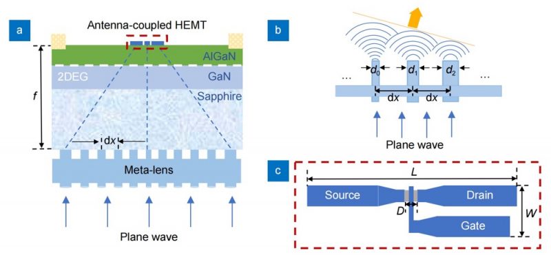
Fig. 1 (a) The integration model of an AlGaN/GaN terahertz detector
The main thickness of the terahertz detector is the sapphire substrate, about 200 μm, with negligible thicknesses of AlGaN and GaN materials. Using the metasurface unit structure array, as shown in Fig. 1(b), the phase control of the beam is realized, and the terahertz wave is focused in the core area of the detector. For terahertz detectors, the asymmetric butterfly antenna is the core area, as shown in Figure 1(c).
When the operating frequency is 1 THz, the width W of the antenna is about 18 μm, the length L is about 74 μm, and the distance D between the antennas is about 1.8 μm, that is, the core area of the terahertz detector is about 18 μm×74 μm.
Considering that when the detector chip and the metasurface lens are back-integrated, if the metasurface lens and the detector substrate are directly coupled, the focal length is too short (f≈200 μm), and more side lobes with large intensity will be generated, which will affect Focus effect.
Therefore, the design focal length of the metasurface lens can be appropriately increased (f=1 mm) by stacking a double-polished sapphire substrate between the metasurface lens and the detector substrate, and then integrated with the detector. After the plane wave passes through the metasurface lens, it passes through the sapphire substrate including the detector substrate and is then incident on the terahertz antenna to focus.
In this paper, based on the transmission phase theory, an all-dielectric array of silicon cylinders is used to realize a terahertz metasurface lens to converge the terahertz beam. According to the principle of medium waveguide, when a beam of a certain cross-section propagates in free space, it will diverge due to diffraction, and a medium with a high refractive index can be used to confine the beam and conduct waveguide transmission.
High-resistance silicon has a very high refractive index (nSi≈3.45), which is the most commonly used material in terahertz lenses, and has extremely low loss in the terahertz range, and the absorption coefficient is less than 0.05cm−1, so the high-resistance silicon material is used. In the metasurface lens unit structure design. At the same time, the metasurface lens has polarization-independent properties due to the symmetry of its array.
Figures 2(a) and 2(b) are schematic diagrams of two metasurface lens unit structures, 2(c) and 2(d) are the side electric field energy distribution diagrams of the 1 THz electromagnetic wave incident on the unit structure along the positive z-axis direction, respectively. The silicon cylinder of the unit structure is a dielectric waveguide, so the energy of electromagnetic waves is mainly confined in the silicon cylinder.
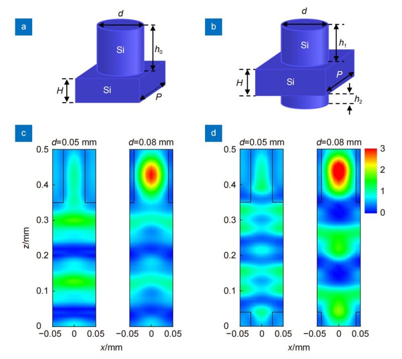
Fig. 2 (a) and (c) show the schematic diagram of single-sided cell structure and its energy distribution; (b) and (d) show the schematic diagram of double-sided cell structure and its energy distribution
As the diameter d of the silicon pillar changes, the effective wavelength of the electromagnetic wave in the waveguide changes accordingly. Compared with the single-sided structure incident plane wave is coupled into the silicon waveguide after passing through the substrate, the double-sided structure incident plane wave is first coupled into the silicon waveguide through the substrate and then coupled into the silicon waveguide again. In the silicon waveguide, it is approximately the fundamental mode (TE mode). The phase and transmittance of the beam after exiting from the silicon waveguide are determined by the transmission characteristics of the fundamental mode of the waveguide.
From the basic principle of two-dimensional slab waveguide, it can be known that the transmission characteristics of the fundamental mode are determined by the refractive index of the medium and the size of the waveguide. For a circular waveguide, the main mode is the TE mode, and the mode eigen equation is
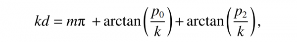
in the formula

Here β is the propagation constant of the guided mode, and the relationship with the waveguide effective refractive index nneff is β=nneff/k0, m is the mode number, which takes a finite number of positive integers starting from 1, where n0 is the waveguide refractive index, n1, n2 is the refractive index of the medium outside the waveguide.
According to the relationship between the effective refractive index nneff of the silicon waveguide and the diameter d, several cells are distributed side by side, with different widths and negligible optical coupling between cells, then the light traveling along the different cells will accumulate proportional to its length The phase shift of , in order to obtain a phase difference of 2π over the subwavelength propagation length, it needs to satisfy:

of which: ∆nneff is the effective refractive index difference between units, so by controlling the diameter d and height h of the silicon waveguide, a series of metasurface unit structures with a phase variation range of 0~2π can be obtained, so that the phase control principle can be used to control the wave array noodle.
3 Metalens Design
Usually, the unit structure of a metasurface lens is to etch a silicon cylinder with the same height on a high-resistance silicon substrate, as shown in Figure 2(a). However, in the actual process preparation process, the aspect ratio of the silicon column is too large, which will cause the silicon column to tilt and collapse. At the same time, as the etching depth increases, the required glue becomes thicker. The photoresist between the pillars can be difficult to clean.
Table 1 The detail parameters of unit structure
| wdt_ID | Parameter | Unit: mm |
|---|---|---|
| 1 | d | 0.03~0.1 |
| 2 | P | 0.1 |
| 3 | H | 0.35 |
| 4 | h0 | 0.15 |
| 5 | h1 | 0.04 |
| 6 | h2 | 0.11 |
In addition, due to the plasma etching principle of high-resistance silicon, as the etching depth increases, the deviation of the verticality of the silicon column will become larger, and the etching height of the silicon column with different duty cycles will also deviate. The effect is that the top is thick and the bottom is thin, and the height is different, which affects the actual aggregation effect of the final product.
In this paper, a double-sided cell structure is designed, as shown in Figure 2(b), by etching symmetrically distributed silicon pillars on both sides of the substrate to reduce the aspect ratio of the silicon pillars and improve the yield and precision of the silicon pillars. The metasurface lens with double-sided structure draws on the principle of anti-reflection coating which is well developed in the visible light range on one side.
If the optical thickness of the anti-reflection layer is a quarter of a certain wavelength, that is, the optical path difference of the reflected beam on the upper and lower surfaces of the silicon pillar is exactly π, and the superposition of opposite vibration directions will reduce the reflected wave of the optical surface for that wavelength.
According to formula (2), to design the anti-reflection layer by using the silicon cylinder, it is necessary to obtain a phase difference that is an integer multiple of π/2 in the subwavelength propagation length, that is, the height of the anti-reflection layer h1=h0/4.
Because the silicon pillars of the anti-reflection layer need to provide a certain phase modulation, the dimensions of the silicon pillars are different at different positions, and a uniform and perfectly matched anti-reflection layer cannot be provided.
By selecting the appropriate height of the silicon cylinder of the anti-reflection layer, the coupling effect of the incident plane wave and the metasurface lens can be improved while changing the phase, the surface reflection loss of the planar silicon substrate can be reduced, and the transmittance of the metasurface lens can be further improved.
The cell structure consists of a cuboid silicon substrate with a period P=100 μm and a silicon cylinder with a total height h0=150 μm. The height of the silicon pillar of the single-sided structure is h0=150μm, the height of the silicon pillar of the anti-reflection layer of the double-sided structure is h1=40 μm, and the height of the front silicon pillar is h2=110 μm, as shown in Fig. 2(a), 2(b).
The finite time domain difference FDTD is used to simulate the cell structure, the boundary condition is set to periodic, the single-sided structure substrate and the double-sided structure anti-reflection layer silicon pillar are respectively incident along the positive direction of the z-axis, and then coupled into the substrate and enter another side after entering the substrate.
The change of the phase is achieved by changing the diameter d of the silicon pillar. Considering the problems of processing accuracy and coupling efficiency, d is parametrically scanned from 30 μm to 100 μm in steps of 1 μm, as shown in Figure 3.
Fig. 3 The phase and transmittance curves of the single and double structure of metasurface lens vary with diameter
The phase modulation characteristics of the double-sided unit structure and the single-sided unit structure are relatively consistent, and the transmission amplitude of the double-sided unit structure is generally larger than that of the single-sided structure, and the advantage is more obvious in the diameter range of 65 μm~80 μm.
At the same time, with the change of diameter d, both structures can achieve 0~2π phase coverage, which meets the design requirements of superlenses.
In order to realize the focusing function of the proposed metasurface structure, transform the terahertz plane wave into spherical wave, and focus at the distance f, the characteristic parameters of each antenna on the surface of the metasurface lens need to be obtained by calculation. According to the relationship between the phase and the optical path, The phase of the focal point to each point on the lens surface must be equal or different by an integer multiple of 2π:
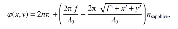
in:
n is an arbitrary integer,
f is the focal length,
λ0 is the wavelength of 1 THz of electromagnetic wave in vacuum,
nsapphire≈3 is the refractive index of sapphire.
Above formula φ(x, y) can calculate the phase value corresponding to each position.
Fig. 4 is a two-dimensional phase discrete distribution diagram of a metasurface lens with a focal length of f=1 mm, an aperture of 3 mm, and an area of 3 mm × 3 mm. The sampling is performed with a square basic unit, and the side length of the square is the period P.
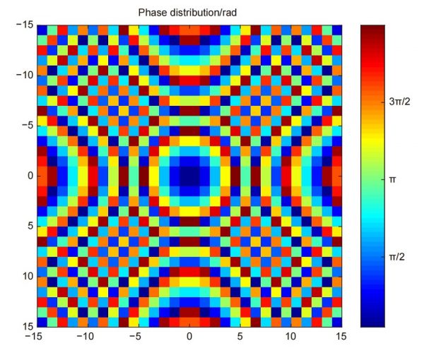
Fig. 4 The two-dimensional phase distribution of metasurface lens
The position of the center point of the phase value is taken as the calculated value, and the corresponding diameter of the silicon column is selected according to the discrete phase value of each position to complete the overall metasurface lens modeling.
The metasurface lens is modeled according to the two-dimensional phase distribution, and Table 2 shows the detailed design parameters.
Table 2 Design parameters of metasurface lens
| wdt_ID | Parameter | / |
|---|---|---|
| 1 | Operating frequency/THz | 1 |
| 2 | Metasurface lens substrate thickness H/mm | 0.35 |
| 3 | Single-sided metasurface lens aperture Ls/mm | 3 |
| 4 | Double-sided metasurface lens aperture Ld/mm | 3 |
| 5 | Design focal length f/mm | 1 |
The numerical aperture NA is a parameter commonly used to describe the performance of a lens. It is related to the focal length and aperture of the lens and is defined as NA=nf sin(arctan(L/f )). Since the metasurface lens is designed to focus in sapphire, nf=nsapphire =3, NA=2.5. The array distribution of the two models is shown in Figure 5. The array rule selects square cells, and the period of each cell is P.
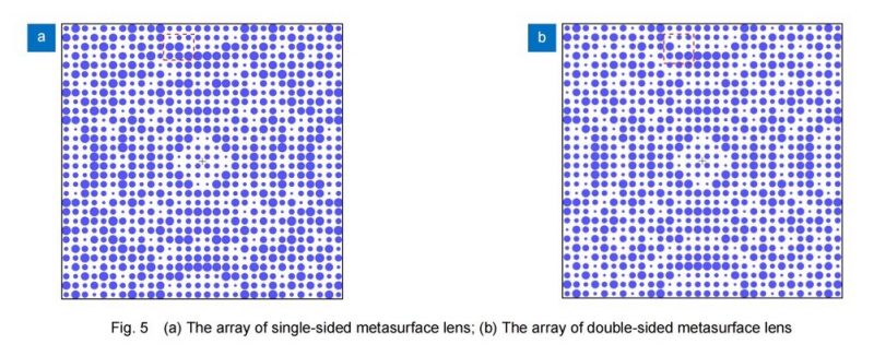
Fig. 5 (a) The array of single-sided metasurface lens; (b) The array of double-sided metasurface lens
According to the scanning parameters of the diameter and phase of the silicon cylinder in Figure 3, the phase modulation characteristics of the two unit structures are relatively consistent, so the difference in the layout of the metasurface lens in Figures 5(a) and 5(b) is small, but there are certain differences. For example the structure shown in the dashed box.
The entire structure is placed in the air in the x and y directions, and the boundaries are set as perfect matching (PML) boundaries, through which the electromagnetic wave passes almost without reflection, and the electromagnetic waves are incident on the silicon substrate of the single-sided metasurface lens along the positive z-axis and a short silicon cylinder of a double-sided metasurface lens, focused in a sapphire medium, as shown in Fig. 1(a).
4 Analysis of results
The electric field distribution of electromagnetic waves entering the sapphire medium through the metasurface lens in space can be seen through the monitor. Figures 6(a) and 6(b) are the single-sided metasurface lens and the double-sided metasurface lens when x=0, respectively. The electric field distribution of the electromagnetic wave propagating in the forward direction of the z-axis. Figures 6(c) and 6(d) are the one-dimensional distribution of the electric field of the two metasurfaces when x=0, y=0.
Figures 6(e) and 6(f) are the electric field distributions of the focal plane of the single-sided metasurface lens and the double-sided metasurface lens, respectively, and Figures 6(g) and 6(h) are the two metasurfaces when y=0 in the focal plane. One-dimensional distribution of the electric field of a surface lens.
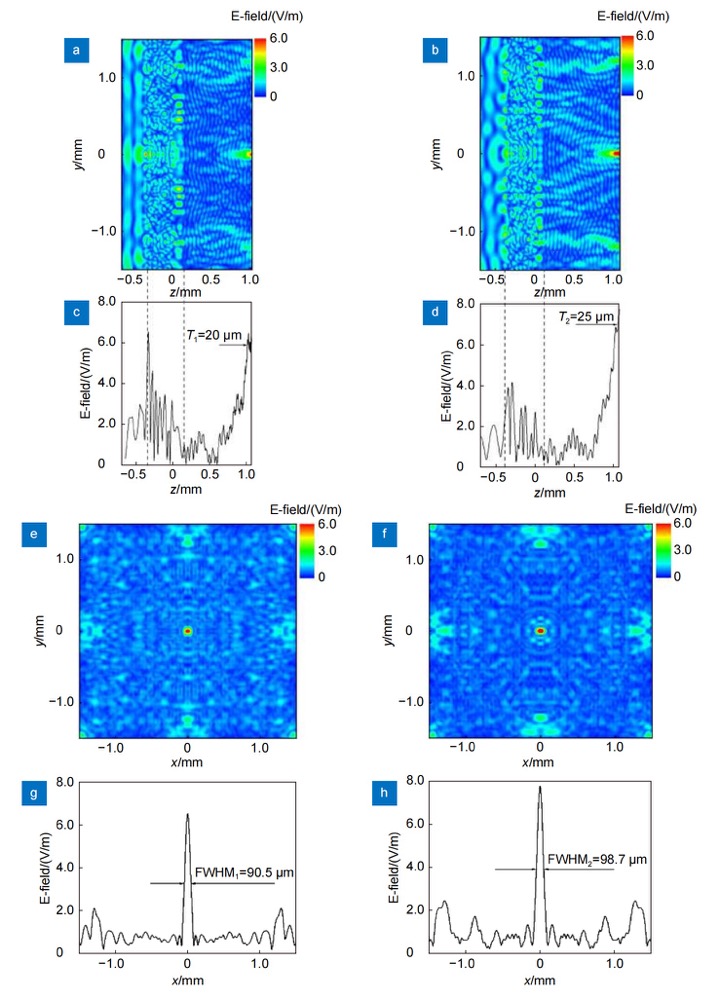
Fig. 6 (a) and (c) show the field intensity distribution on the y-z plane and one-dimensional distribution on the y=0 of a single-sided structure when x =0 ; (b) and (d) are the field intensity distribution on the y-z surface when x=0 and one-dimensional distribution when y=0 of the double-sided metasurface lens; (e) and (g) are the field intensity distribution on the x-y plane and the one-dimensional distribution on y=0 when z=1.026 mm of the single-sided metasurface lens; (f) and (h) are the field intensity distribution on the x-y plane and the one-dimensional distribution on y=0 when z=1.067 mm of the double-sided metasurface lens
The focusing effect of the metasurface lens of the two structures is obvious (Fig. 6(a~d)), and the field strength reaches the maximum value near z=1 mm, forming an energy peak.
However, the actual focal length of the two metasurface lenses deviates slightly from the theoretical design value f=1 mm, which are 876 μm and 962 μm respectively. The main reason for the deviation is the discretized arrangement of the surface unit structure of the metasurface lens, which cannot be done to full-phase continuous sampling.
The 1 dB mismatch tolerance is an important index to measure the optical coupling system, and it is also an important criterion to solve the coupling packaging problem.
According to the field intensity distribution of the y-z plane, the tolerances T1 and T2 of the metasurface lens along the z-axis are 20 μm and 25 μm, respectively, so the allowable range of thickness error of sapphire in the actual preparation process is about ±25 μm.
The light spot focused by the metasurface lens at the focal length is shown in Fig. 6(e~f). The results of the two structures are not very different, and the focal spot shape is better and symmetrical.
By calculation, the full width at half maximum (full width) of the focused spot of the two metasurface lenses width at half maximun, FWHM) are 90.5 μm and 98.7 μm, respectively, which are comparable to the size of the terahertz antenna, so the terahertz wave can be well focused on the antenna with the detector.
The maximum value of the electric field strength of the terahertz wave at 1 THz increases to 6.5 times and 7.8 times that of the incident plane wave through the two metasurface lenses, respectively, and the average electric field strength in the core region increases to 5.7 times and 6.6 times that of the incident plane wave, respectively. The electric field energy density is proportional to in the square of the electric field strength.
Therefore, the terahertz wave is radiated to the terahertz detector through the metasurface lens, and the electric field energy density in the core area is increased by about 32 times and 44 times, respectively, and the energy density of the double-sided metasurface lens is about 37.5% higher than that of the single-sided metasurface lens.
The working efficiency of the double-sided metasurface lens is better than that of the single-sided metasurface lens, because the reflection loss of the flat silicon substrate is large, and the terahertz wave incident on the silicon substrate cannot be effectively utilized, and the working efficiency of the metasurface is reduce.
For the metasurface lens with double-sided structure, one side can act as an anti-reflection layer while changing the phase, thereby further improving the working efficiency of the metasurface lens.
We calculated the focusing efficiency of the two metasurfaces, and defined the ratio of the energy in the square area with the focal spot in the focal plane as the center and three times the half-height width as the side length to the energy incident on the metasurface lens as the focusing efficiency of the metasurface lens, The focusing efficiencies of the single-sided metasurface lens and the double-sided metasurface lens are 8.3% and 10.8%, respectively. Table 3 is a comparison of the performance of different types of terahertz meta-lenses in recent years.
Table 3 Performance comparison of metasurface lens in terahertz band
| Material and structure | Operating frequency/THz | Numerical aperture | FWHM of focal spot/μm | Focusing efficiency/% | ||||
| V-shaped antenna (Au) + silicon substrate | 0.75 | 0.71 | 270 | 1 | ||||
| V-shaped antenna (Cu) + silicon substrate | 1.1 | 0.78~0.95 | 165~206 | 2.7~5.2 | ||||
| Square ring groove (Al) - medium (BCB) - square ring groove (Al) | 0.84 | 0.41 | Focal spot diameter 450 | Electric field gain 5.2 | ||||
| Cross Silicon Cross | 3.11 | 0.16 | 630 | 24 | ||||
| Silicon square column (double-sided) | 2.52 | 0.92 | 47.5 | 24.2 | ||||
| Silicon cylinder (single side) | 1 | 2.50 | 90.5 | 8.3(Electric field gain 6.5) | ||||
| Silicon cylinder (double-sided) | 1 | 2.50 | 98.7 | 10.8(Electric field gain 7.8) | ||||
| Au: Gold; Cu: Copper; Al: Aluminum; BCB: Benzocyclobutene | ||||||||
Compared with metal-structured meta-lenses, the work in this paper has higher focusing efficiency for terahertz waves, but compared with other all-dielectric meta-lenses, the focusing efficiency is higher. There is no clear advantage in efficiency.
Because the metasurface lens in this paper is designed to focus in the sapphire medium in order to better integrate with the terahertz detector, the lens aperture is the size of the detector substrate, which increases the numerical aperture. The increase in side lobe energy, as shown in Fig. 6(a–h), leads to low focusing efficiency.
At the same time, when designing the anti-reflection layer, the feasibility of the process preparation has been comprehensively considered. Although it has a certain anti-reflection effect compared to the planar silicon substrate, it does not achieve uniform anti-reflection phase modulation and cannot achieve complete anti-reflection effect.
We calculated a silicon lens with a diameter of 3 mm. At an operating frequency of 1 THz, the mean gain of the electric field in the core region is 19 times, the half-height at the focal spot is 99.3 μm, and the focusing efficiency reaches 86.9%. The suppression of side lobes The effect is better.
The next work will further optimize the aperture and focal length of the metasurface lens based on the parameters of the terahertz detector, and suppress the side lobes, so as to improve the focusing efficiency of the metasurface lens and be better applied to the terahertz detector.
In order to explore the dispersion characteristics of the designed metasurface lens, a plane wave with a frequency range of 0.9 THz~1.1 THz was incident on a double-sided metasurface lens with an operating frequency of 1 THz, and according to the focusing principle formula φ(x, y), the frequency and focal length for theoretical calculations.
As shown in Fig. 7, in the range of small frequency change, the focal length of the metasurface lens is relatively stable, and the overall trend increases with the increase of frequency, which is close to the trend of the theoretical calculation value.
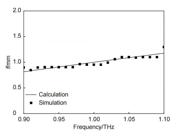
Fig. 7 Dispersion characteristics of double-sided metasurface lens
The main reason for the dispersion of metasurface lenses is that the unit structure is designed depending on the wavelength of the incident wave, and the phase modulation has frequency-dependent characteristics.
In the follow-up work, in order to realize the broadband operation of the metasurface lens, on the basis of not changing the unit structure design, the metasurface can be arrayed by the achromatic structure method, and the incident waves of different frequencies can be arranged at the same position by the composite splicing method. focus, but the focusing efficiency will be reduced accordingly.
At the same time, the metasurface lens is designed with a wavelength-independent unit structure, such as the geometric phase type. The phase change of the unit structure is only related to its geometric position, which can make the lens have frequency-independent characteristics.
However, the geometric phase element will change the polarization state of the electromagnetic wave, and the polarization characteristics of the incident wave need to be considered when integrating with the terahertz detector.
5 Conclusion
In this paper, a series of high-resistance silicon cylindrical unit structures are designed, and the phase coverage of 0~2π and high transmittance are achieved by changing the size of the silicon column.
A metasurface lens with a thickness of only 500 μm is designed by using the silicon cylindrical unit structure, and it is used in a terahertz detector with a center frequency of 1 THz, which can make the focal spot size and wavelength in the same order of magnitude. The working efficiency of the metasurface lens is better than that of the single-sided metasurface lens, and the electric field energy density at the terahertz antenna is increased to 44 times that of the incident plane wave.
Compared with the traditional hyperhemispheric terahertz silicon lens, the small size and thin thickness of the metasurface lens are more conducive to integration, and have great prospects for reducing the complexity of the terahertz system and improving the responsivity of the detector. And miniaturization provides a new idea.
Since the current metasurface lens generates more sidelobes after focusing, the focusing efficiency is low. In the future, the material and unit structure of the metasurface lens will be further optimized to improve the focusing efficiency and electric field energy density.