Ion Beam Polishing Process of Off-Axis Parabolic Mirror
optical design; ion beam polishing; off-axis parabolic mirror; thermal effects; variable beam diameter
Abstract
Aiming at the problems of thermal effect accumulation and iterative processing efficiency in the process of off-axis parabolic mirror ion beam modification, a method is proposed to combine batch machining with variable beam diameter machining, which divided the total removal amount according to a certain proportion, and the experimental exploration is carried out by using this method.
The spherical mirrors with an aperture of 110 mm, a radius of curvature of 1732.7 mm, an initial surface peak-valley value (PV) of 0.525λ (l=632.8 nm) and a root mean square (RMS) value of 0.025λ are polished in batches. The off-axis parabolic mirrors with vertex radius of curvature of 1728 mm, off-axis of 85 mm, PV of 0.36λ and RMS of 0.029λ are obtained. Based on the analysis of the experimental process and results, it is proved that the batch machining method can effectively eliminate the thermal effect in the ion beam machining process, and the local finishing method with variable beam diameter can reduce the number of iterative machining and improve the machining efficiency.
1 Introduction
Off-axis parabolic mirrors are commonly used optical components in optical instruments, and have been widely used in off-axis reflective collimators and off-axis double/triple mirror systems. The ion beam polishing technology is a high-precision and deterministic modification technology.
It uses a stable non-contact ion beam to replace the contact polishing pad, which can effectively avoid the subsurface damage of the polishing pad and the processing element during the contact polishing process. , which can effectively solve the insufficient edge removal caused by insufficient contact between the polishing pad and the processing element at the edge, as well as the removal uncertainty caused by the wear of the polishing pad, the non-contact ion beam polishing technology has higher surface polishing and modification accuracy. However, in the process of ion beam modification, multiple iterative processing is usually required to improve the surface shape accuracy of the component to be processed. Therefore, the ion beam polishing technology has higher surface shape processing accuracy, but the processing efficiency is low.
In 2016, Tang Wa of Changchun Institute of Optics, Fine Mechanics and Physics conducted a lot of research work on the removal model and process of ion beam polishing large-aperture aspheric surfaces, established and improved the process operation flow of ion beam polishing large-aperture aspheric surfaces, And completed a number of high-precision polishing of large-diameter off-axis aspheric mirrors, including the polishing of Φ1450 mm silicon modified layer off-axis aspheric surface. After 30h of processing, the root mean square (RMS) value of surface shape error is 50.912nm reaches 8.785nm.
In 2017, Yin Xiaolin of Changchun Institute of Optics, Fine Mechanics and Physics conducted a lot of research work on ion beam modification equipment and processes for spatially complex optical surfaces, and proposed a combined machining strategy of small grinding head and ion beam, which can The introduction of medium and high frequency errors is effectively reduced, and the processing cycle of the entire optical element is shortened while improving the final processing accuracy of the ion beam.
Yin Xiaolin conducted an ion beam modification experiment on a high-steep fused silica spherical mirror with a diameter of 100mm. The final RMS value of the surface shape of the optical element converged from the initial 0.032λ to 0.014λ (λ= 632.8nm), and the convergence ratio reached 2.3, it shows that the proposed machining strategy has high surface machining accuracy.
In 2018, Li Zhigang et al. of Chengdu Precision Optical Engineering Research Center proposed a computer-controlled multi-grinding head combined polishing technology, which can effectively control the mid-frequency error (PSD1) of aspherical components, and finally Φ460 mm off-axis parabolic components. The PSD1 value of the surface shape decreased by nearly 70% compared with the previous one, reaching 2.835nm, the peak-to-valley (PV) value reached 0.16λ, and the RMS value reached 0.02λ.
In this paper, the ion beam polishing process based on off-axis parabolic mirror is studied, and the process experiments are all carried out on the ion beam polishing machine independently developed by our research group.
In this paper, aiming at the problem that the thermal effect affects the ion beam modification accuracy during the ion beam processing, a certain proportion of the total processing time is allocated to be processed in batches to eliminate the influence of the thermal effect; for the problem of low convergence efficiency of the ion beam polishing surface , a variable beam diameter processing method based on ion beam is proposed, that is, a staged processing method of original diameter processing, small beam diameter processing, and small beam diameter local high point processing.
2 Solving the closest spherical surface
At present, researchers are generally looking for a matching spherical surface to process off-axis parabolic mirrors. In order to characterize the processing difficulty of aspherical components, the concept of asphericity is proposed, that is, the deviation value between spherical and aspherical surfaces. The greater the asphericity, the more difficult it is to process aspherical components, and the higher the time and cost.
In this paper, the coordinate system of the off-axis parabolic mirror and the machining coordinate system are established by means of transforming the coordinate system. That is, after the original coordinate system undergoes coordinate translation and rotation, a new coordinate system with the center of the off-axis parabolic mirror as the origin is obtained. The horizontal axis is the tangent of the new origin coordinate system on the off-axis paraboloid. The vertical axis is the vertical line of the new origin coordinate system on the off-axis paraboloid, coordinate transformation, as shown in Figure 1, where P is the center point of the off-axis parabolic mirror, φ is the angle between the normal of the off-axis parabolic mirror and the axis of symmetry.
Fig.1 Schematic of coordinate transformation of off-axis parabolic mirror
The equation of the original parabola is
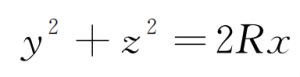
equation 1
In the formula: (x, y, z) is the original coordinate; R is the radius of curvature of the vertex of the paraboloid. The transformation relation of translation transformation can be expressed as
equation 2
In the formula: (x’, y’, z’) are the transformation coordinates; (a, b) are the horizontal and vertical coordinates of the point P. The transformation relationship of the rotation transformation can be expressed as
equation 3
Substituting equations (2) and (3) into equation (1), we can get
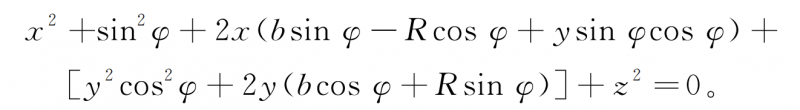
equation 4
The abscissa of each point of the off-axis parabolic mirror can be obtained by formula (4). Taking the calculation formula of the off-axis paraboloid as the criterion, searching and optimizing according to the search algorithm flow in Figure 2, the trimming amount closest to the spherical surface and the material can be obtained.
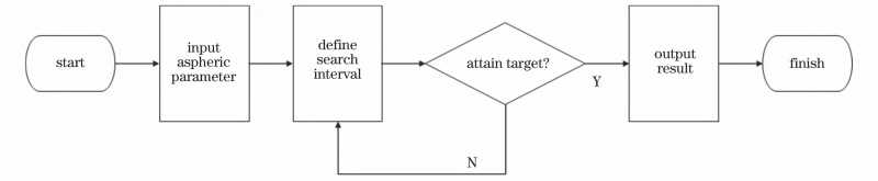
Fig. 2 Flow chart of search algorithm closest to sphere
At the same time, according to the different aspheric surfaces, the conic coefficients are changed and the higher-order terms are added, and the search algorithm is more universal at this time.
After calculation, an off-axis parabolic mirror with a diameter D of 110 mm, a radius of curvature R of 1728 mm, and an off-axis amount h of 85 mm is obtained.
The simulation results are shown in Fig. 3, in which Fig. 3 (a) is the 3D sag height simulation graph of the off-axis paraboloid, Fig. 3 (b) is the 3D sag height simulation graph closest to the spherical surface, and Fig. 3 (c) is the spherical off-axis paraboloid. Figure 3 (d) is the asphericity curve. After solving, the radius of curvature closest to the sphere is 1732.7mm, and the maximum asphericity is 2.3μm, that is, the maximum removal thickness of the edge is 2.3μm, and the total volume removal is 5.32mm3.
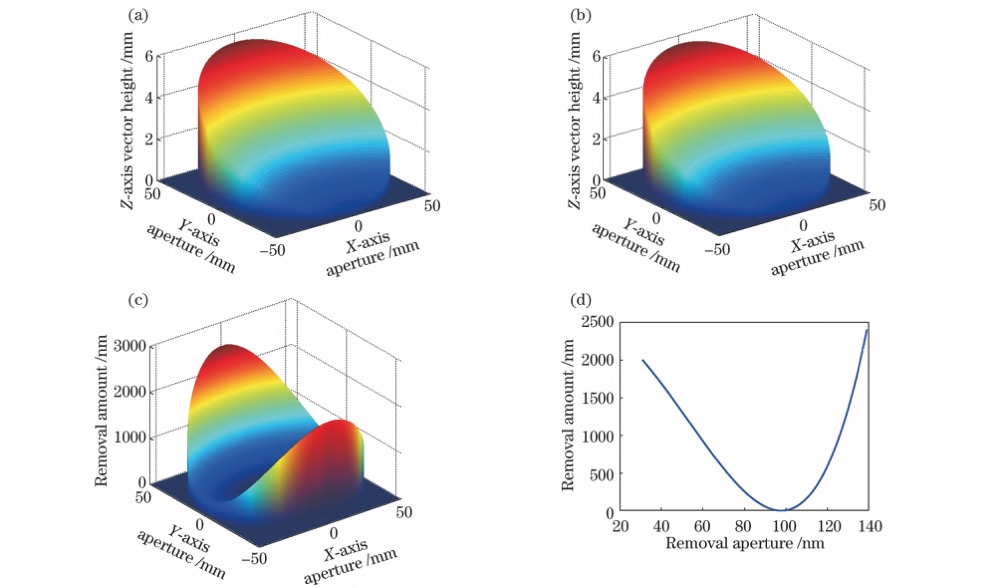
Fig.3 Three-dimensional simulation results of off-axis parabolic mirror. (a) Vector height of off-axis paraboloid; (b)vector height of best fitting sphere; (c) removal amount of sphere turning off-axis paraboloid; (d) asphericity curve
The initial spherical mirror is shown in Figure 4.
Fig.4 Initial spherical mirror
3 Exploration experiment of suppressing thermal effect during ion beam polishing
In the process of ion beam processing, high-speed ions impact on the surface of optical components, and energy transfer occurs with the atoms on the surface, and most of the energy of the incident ions is converted into thermal energy, which will lead to a rapid increase in the temperature of the optical surface processing part.
If the residence time of the machining part is too long or the superposition time is too long, the local heating will be too fast, resulting in a nonlinear change of the removal rate of the machining part, which will affect the accuracy and reliability of the ion beam surface machining. Therefore, effective measures must be taken to suppress this thermal effect in the ion beam processing technology, so as to ensure the certainty of the ion beam and the reliability of the processing.
According to the process parameters for stable operation of the ion source (Table 1), the line scan experiments were carried out on a K9 optical plane element with a diameter of 50 mm.
Table 1 Process parameters for stable operation of ion source
| wdt_ID | Parameter | Value |
|---|---|---|
| 1 | Background vacuum / (10^-3 Pa) | 5.3 |
| 2 | Operating vacuum / (10^-2 Pa) | 4.2 |
| 3 | Radio frequency power / W | 200 |
| 4 | Screen grid voltage /kV | 0.9 |
| 5 | Accelerator grid voltage / V | 100 |
| 6 | Duty cycle / % | 90 |
| 7 | Gas flow / (mL·min^-1) | 50 |
| 8 | Working distance / mm | 95 |
Increasing the stacking spacing during the experiment can make the ion beam process a strip on the optical element similar to the effect of the single-point etching experiment. The surface subtraction diagram of the K9 optical element is shown in Figure 5, and the reading result of the MATLAB software is shown in Figure 6.
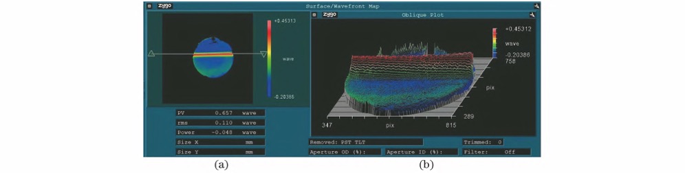
Fig. 5 Surface shape subtraction diagram after lines canning processing. (a) 2D diagram; (b) 3D diagram
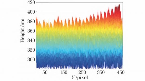
Fig.6 Etching depth diagram on MATLAB
It can be seen from Figure 6 that the ion beam etching depth on the element shows a gradually increasing trend from left to right, where the superposition removal rate of the leftmost point is 1176 nm/min, and the superposition removal rate of the rightmost point is 1263nm/min.
In the early stage of the experiment, the processing temperature of the components has not reached the equilibrium point, so the phenomenon of low removal rate in the early stage occurs. With the increase of processing time until the middle and late stages of processing, the removal rate gradually increases.
If the removal rate of pre-processing is used to calculate the residence time, the phenomenon of over-removal in the post-processing of the experiment will occur due to the low removal rate; if the removal rate of post-processing is used to calculate the residence time, it will cause the removal rate in the early stage to be larger than the actual one, resulting in the phenomenon of under-removal in the early stage.
To sum up, the above phenomenon is more serious when dealing with optical elements that have a long residence time due to a large amount of processing removal.
The thermal effect will lead to a nonlinear change in the removal rate. For this reason, this paper proposes a batch processing method.
That is, when the total processing time remains unchanged, the total processing time is divided according to a certain proportion to achieve the purpose of multiple processing.
The advantage is that the first processing can ensure a certain amount of removal and at the same time make the temperature of the sample reach a relatively balanced state, and then carry out precision trimming processing in batches to reduce the thermal effect during the modification process, so as to achieve the purpose of deterministic removal.
The surface scanning experiment was carried out using an ion beam with an aperture diameter of 8 mm.
Figure 7 is the surface map obtained after one-time surface scanning experiment in the total dwell time.
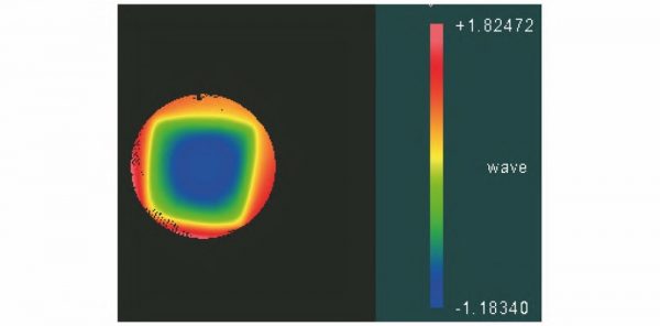
Fig.7 Surface diagram of one-time surface scanning
Figure 8 is the surface map obtained after subdividing the total dwell time into three batches for the surface sweep experiment.
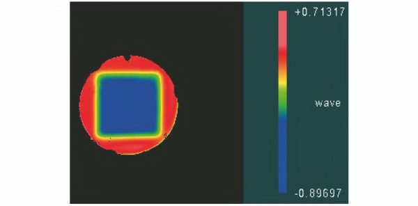
Fig.8 Surface diagram of batch sub-surface scanning
It can be seen from Figure 7 and Figure 8 that the one-time surface sweep experiment has obvious under-removal phenomenon, and batch processing effectively eliminates the thermal effect during processing, so it is more in line with the expected processing effect.
4 Experiment of off-axis parabolic mirror ion beam machining
4.1 Spherical off-axis parabolic machining
Ion beam polishing is a technology based on atomic-level physical sputtering. It uses a specific removal function to bombard the surface of the optical element for a certain period of time according to the preset addition path, so as to achieve the purpose of atomic-level removal, and then realize the correction of the surface shape. The polishing accuracy mainly depends on the removal function and the dwell time.
After the initial surface shape and removal function of the optical element are known, how to use these two factors to determine the dwell time to minimize the surface shape residual is a key factor affecting the surface shape accuracy.
In this paper, the algorithm accumulated in the early stage of the laboratory is used to solve the residence time.
The processing sample of the spherical off-axis parabolic mirror is a concave spherical mirror with a diameter of 110mm, a radius of curvature of 1732.7mm, and a material of K9. A ZYGO interferometer is used to detect the initial spherical shape, which is superimposed with the solved material removal to calculate the dwell time.
According to the previous process experiments, the peak removal rate of the ion beam without diaphragm is 386.5 nm/min, the removal function distribution parameter is 5 mm, and the stacking spacing is set to 7.5 mm.
Due to the large amount of machining removal and long theoretical residence time in the local area of the spherical off-axis parabolic mirror, batch processing must be adopted to effectively suppress the influence of thermal effects.
In order to determine the time for the first batch processing of the actual sample, it is necessary to verify the temperature equilibrium point of the sample, so a plane optical element with a diameter of 110mm was selected for the equivalent surface scan experiment, and a thermocouple was placed on the sample for measurement. temperature, monitor the processing time in a steady state of temperature rise.
That is, the temperature equilibration time, the temperature equilibration time of the planar optical element obtained by the experimental process is 72 minutes, so the time for the first batch processing should not be less than the temperature equilibration time, and the theoretical residence time of the spherical off-axis parabolic mirror longer, about 13h. Therefore, the ratio of batch processing time was set to 1:2:7.
Fig. 9(a) and Fig. 9(b) are the surface shape errors of the initial spherical surface, Fig. 9(c) is the material removal stacking amount, Fig. 9(d) is the simulation result of 10% dwell time, Fig. 9(e) is the simulation result of 20% dwell time, and Fig. 9(f) is the simulation result of 70% dwell time.
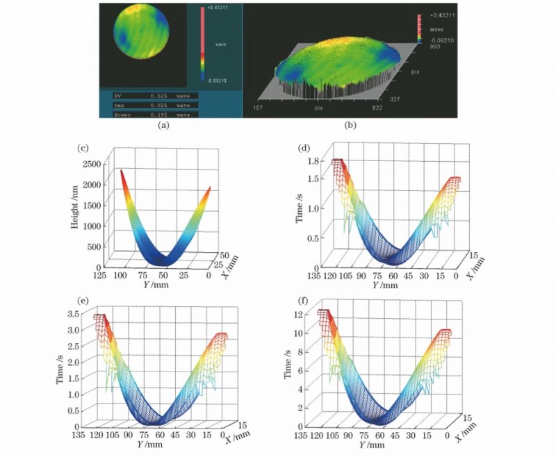
Fig.9 Simulation results of batch machining of spherical off-axis paraboloid mirror. (a)Two-dimensional distribution of initial spherical error of concave spherical mirror; (b) three-dimensional distribution of initial spherical error of concave spherical mirror; (c)total material removal; (d)10% residence time; (e)20% residence time; (f)70%residence time
The batch processing method was used for three iterations, and the aberration-free point method in the zero-position interference method was used to detect the off-axis parabolic mirror.
Since the F-number of the off-axis parabolic mirror to be tested is 7.8, a standard spherical mirror with an F-number of 7.1 was selected for the experiment.
Since the standard spherical wave emitted by the interferometer coincides with the focus of the off-axis parabolic mirror to be measured, the spherical wave becomes a plane wave after being reflected by the off-axis parabolic mirror, and the standard plane mirror is placed near the focus to avoid cutting light. Adjust The deflection angle is until the test beam returns from the collimated original path after passing through the standard plane mirror, and interferes with the standard spherical wave. At this time, the surface shape error of the off-axis parabolic mirror to be measured can be measured.
The detection optical path is shown in Figure 10, the real object of the detection site is shown in Figure 11, and the detection surface shape is shown in Figure 12. Figure 12(a)~12(c) are the surface shape detection results of three iterative processing respectively. After three iterations, the RMS value of the off-axis parabolic mirror surface shape error converges to 0.103λ, and the PV converges to 0.837λ.

Fig.10 Schematic of detection light path of off-axis parabolic mirror

Fig.11 Inspection diagram of off-axis parabolic mirror
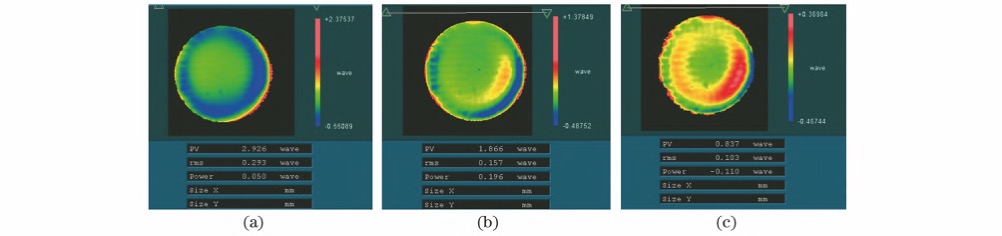
Fig.12 Surface shape detection results of off-axis parabolic mirror after three iterations. (a) Test results after 1st processing; (b) test results after 2nd processing; (c) test results after 3rd processing
4.2 Small beam diameter ion beam processing
Errors in different frequency bands have different effects on the surface shape, and in the ion beam processing process, only the mid- and low-frequency errors can be effectively removed. There are generally two methods of changing the beam diameter of the ion beam:
- The first is to design grids with different curvatures and apertures, and adjust the parameters of the ion source, so as to achieve the purpose of changing the beam diameter of the ion beam;
- The second is to design diaphragms with different apertures under the original curvature and aperture, that is, to block the ion beam exit and change the beam diameter externally, so as to achieve the purpose of reducing the beam diameter.
The operation of the first method is more complicated, and different grid systems need to be designed, which has a high utilization rate of energy, but the process of replacing the grid system is cumbersome, and replacing the grid system for different needs cannot guarantee the same installation position twice. It will also cause errors in the removal function, which requires a large number of repeated process experiments to verify, so the process is time-consuming, labor-intensive and costly.
The second method is to design apertures of different sizes and target distances of different heights on the basis of the original structure, so that the beam diameter of the ion beam can be reduced. However, the second method was adopted by our research group to carry out ion beam trimming processing with small beam diameter.
Considering that the beam diameter of the ion beam is too small, more ion beam energy will be intercepted, and the lower the removal rate of the ion beam will cause the processing time to double and the processing efficiency to decrease. Therefore, an aperture with an aperture of 8 mm is used to remove the function. The obtained process experiment is shown in Figure 13.
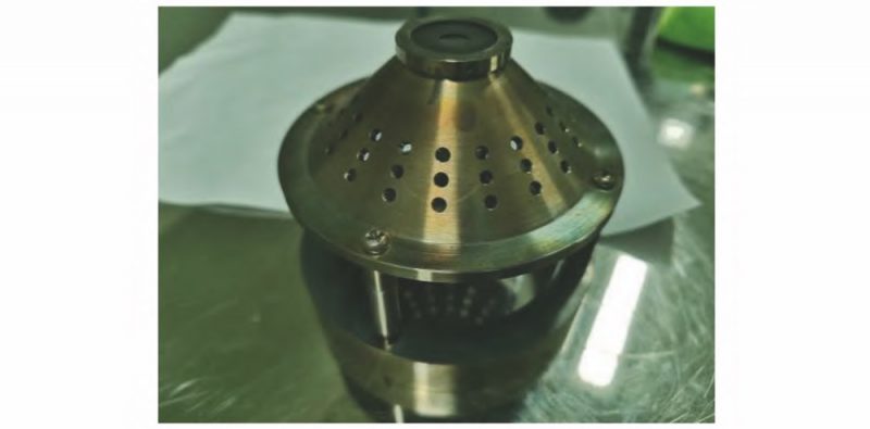
Fig.13 Physical diagram of ion source aperture
According to the process experiment, the peak removal rate of the 8mm aperture is 325.4nm/min, the distribution parameter of the removal function is 2.38mm, and the stacking spacing is set to 3.57mm. After calculating the dwell time, the small beam diameter ion beam is modified. , the surface shape PV of the off-axis parabolic mirror after processing is 1.187λ, and the RMS value is 0.064λ. The test results are shown in Figure 14.
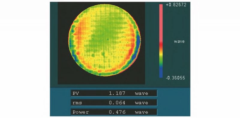
Fig.14 Test results of surface shape after machining of small beam diameter
4.3 Deterministic processing of small beam diameter local high spot ion beam
The local high point ion beam processing method is to take a base surface on the original surface shape, and then only modify the high point higher than the base surface, so that the overall surface shape error can be reduced to the base surface level.
This method is suitable for the base level of most parts of the component where the base level converges around a value, and a base level can be set slightly lower or higher than the convergence extreme value according to the requirements, which can make the overall surface shape converge quickly again.
Based on the above principles, this paper needs to find a datum plane as a suitable datum. As shown in Figure 15(a), the RMS value of the central area of the off-axis parabolic mirror basically converges to within 10 nm, and the accuracy can reach λ/50, which fully meets the requirements of the technical specifications.
At this time, as long as the surface shape values of other regions are close to this value, the entire off-axis parabolic mirror can have very high surface shape accuracy. Make a ruler in the entire surface error distribution map, and adjust it by moving up and down to find the maximum PV (not limited to the horizontal direction, you can make a ruler at any angle to find the maximum PV), as shown in Figure 15(b).
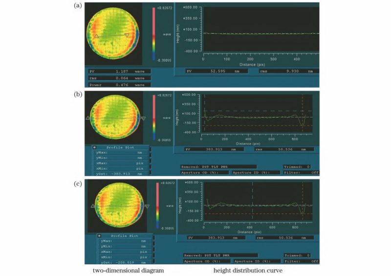
Fig.15 Analysis results of local high point ion beam modification base surface. (a) Surface shape detection and pick-up figure l; (b) surface shape detection and pick-up figure 2; (c)surface shape detection and pick-up figure 3
It can be seen from Figure 15(b) that the surface error PV of the off-axis parabolic mirror is 383.913 nm. MetroPro software has its own standard for the baseline, that is, the height is 200nm, and the surface data is retained from the valley value to the baseline, and the surface data above the baseline is the surface data to be processed, as shown in Figure 15(c).
The local high point ion beam processing method with small beam diameter needs to add the selection of the base value to the dwell time solution algorithm. After regularization, the base value of 200 nm is selected to solve the dwell time. The results are shown in Figure 16.
Fig.16 Simulation results of regularized base surface removal
The surface shape detection results after processing are shown in Figure 17. It can be seen from Fig. 17 that after processing, the surface error PV of the off-axis parabolic mirror is 0.36λ, and the RMS value is 0.029λ. Finally, the ion beam precision trimming and polishing of the off-axis parabolic mirror is realized.
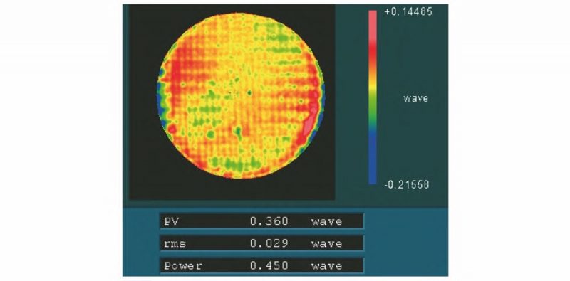
Fig.17 Detection results of final surface shape of off-axis parabolic mirror
5 Conclusion
In this paper, through the exploration of the technology of suppressing the thermal effect during the ion beam polishing process, the experiment verifies the effectiveness of dividing the total processing time into multiple batches according to a certain proportion to suppress the thermal effect.
Calculate the closest spherical surface to the off-axis parabolic mirror with the diameter D= 110mm, the vertex curvature radius R=1728mm, and the off-axis amount h= 85mm, and obtain the curvature radius R=1732.7mm closest to the spherical surface.
The initial spherical surface was obtained by the traditional polishing process, and the ion beam polishing was used for batch processing for three iterations.
Finally, the ion beam precision polishing of the off-axis parabolic mirror with the surface error PV of 0.36λ and the RMS value of 0.029λ is realized.
The obtained results effectively improve the ion beam machining accuracy and process efficiency of the off-axis parabolic mirror, and provide a reliable process method for other types of aspheric ion beam machining.