Measuring and Calculating Visual Defects
There are seven main sources that address measuring, calculating, and evaluating visual defects. These sources include three military specifications and two ISO standards, the latter of which are part of
• ISO 10110,
“Optics and photonics—Preparation of drawings for optical elements and systems”:
• MIL-PRF-13830B:1997 (which replaced MIL-O-13830A:1963),
“Optical Components for Fire Control Instruments; General Specification Governing the Manufacture, Assemble and Inspection of;”
• MIL-C-48497 (1980),
“Coating, Single or Multilayer, Interference: Durability Requirements for;”
• MIL-F-48616 (1977),
“Filter (coatings), Infrared Interference: General Specification for;”
• ISO 10110-3:1996,
“Material imperfection—Bubbles and Inclusions;”
• ISO 10110-7:2008,
“Surface Imperfection Tolerances;”
• ISO 14997:2011,
“Optics and photonics – Test methods for surface imperfections of optical elements;” and
• ANSI/OEOSC OP1.002-2009, “Optics and Electro-Optical Instruments—
Optical Elements and Assemblies—Appearance Imperfections.”
Customers may ask for a different and legal requirement for their needs.
The result may also be a combination of special requirements with measuring and calculation according to the stated standards.
Scratches and digs
The paragraphs in Figs. below, reprinted from MIL-PRF-13830B, are relevant when dealing with scratches and digs.
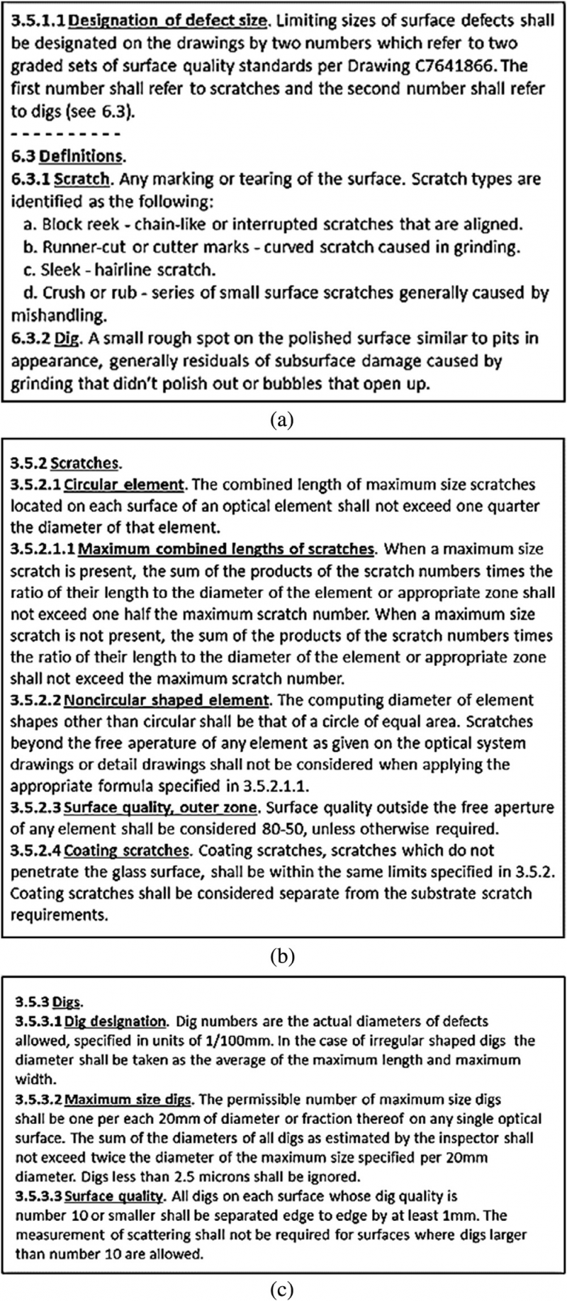
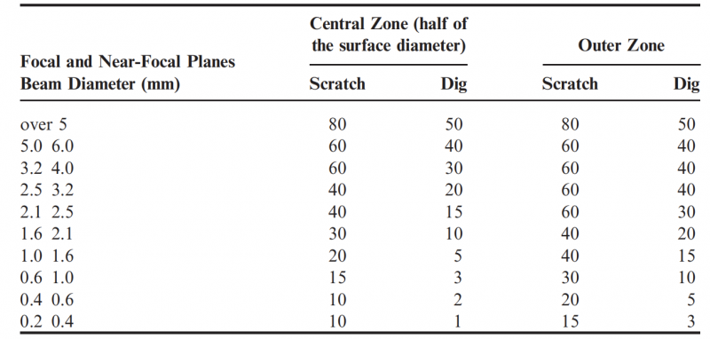
Table below also from MIL-PRF-13830B, shows the scratch and dig numbers for the central zone (half of the surface diameter) and the outer zone beam diameter (mm), respectively, referring to the focal planes and near-focal planes (the table represents general recommendations, and designers are free to determine different definitions that fit to the system’s needs).
Surface defects on optical elements (scratches and digs) are designated by two numbers. The first number refers to scratch width, and the second number refers to dig diameter. For example, 80-50 means that the maximum allowable width of a scratch is 80 and the maximum allowable dig diameter is 50 by comparing both numbers to the quality standards, per drawing no. C7641866.
Note that the combined length of the maximum-size scratches located on each surface of a circular element should not exceed one-fourth of the surface diameter. Further notes:
- To calculate surfaces other than circular ones, the computing diameter should be that of a circle of equal area.
- Scratches beyond the free aperture (i.e., clear aperture, or CA) of any surface of any element should not be considered when calculating the equal value of the existing scratches.
- The surface quality outside the free aperture of any element should be considered 80-50 unless otherwise required.
- Coating scratches should be considered separately from the substrate scratch requirements, and the substrate scratches should have the same size unless otherwise required.